- 您现在的位置:买卖IC网 > Sheet目录1993 > DS1337S+C01 (Maxim Integrated Products)IC RTC SERIAL 2WIRE LP 8-SOIC
DS1337 I
2C Serial Real-Time Clock
PIN DESCRIPTION
PIN
8
16
NAME
FUNCTION
1
—
X1
2
—
X2
Connections for a Standard 32.768kHz Quartz Crystal. The internal
oscillator circuitry is designed for operation with a crystal having a specified
load capacitance (CL) of 6pF. For more information about crystal selection
and crystal layout considerations, refer to
Application Note 58: Crystal
Considerations with Dallas Real-Time Clocks. An external 32.768kHz
oscillator can also drive the DS1337. In this configuration, the X1 pin is
connected to the external oscillator signal and the X2 pin is floated.
3
14
INTA
Interrupt Output. When enabled,
INTA is asserted low when the
time/day/date matches the values set in the alarm registers. This pin is an
open-drain output and requires an external pullup resistor. The pull up
voltage may be up to 5.5V, regardless of the voltage on VCC. If not used, this pin
may be left floating.
4
15
GND
Ground. DC power is provided to the device on this pin.
5
16
SDA
Serial Data Input/Output. SDA is the input/output pin for the I
2C serial
interface. The SDA pin is open-drain output and requires an external pullup
resistor.
6
1
SCL
Serial Clock Input. SCL is used to synchronize data movement on the serial
interface.
7
2
SQW/
INTB
Square-Wave/Interrupt Output. Programmable square-wave or interrupt
output signal. It is an open-drain output and requires an external pullup
resistor. The pull up voltage may be up to 5.5V, regardless of the voltage on VCC.
If not used, this pin may be left floating.
8
3
VCC
DC Power. DC power is provided to the device on this pin.
—
4–13
N.C.
No Connect. These pins are not connected internally, but must be
grounded for proper operation.
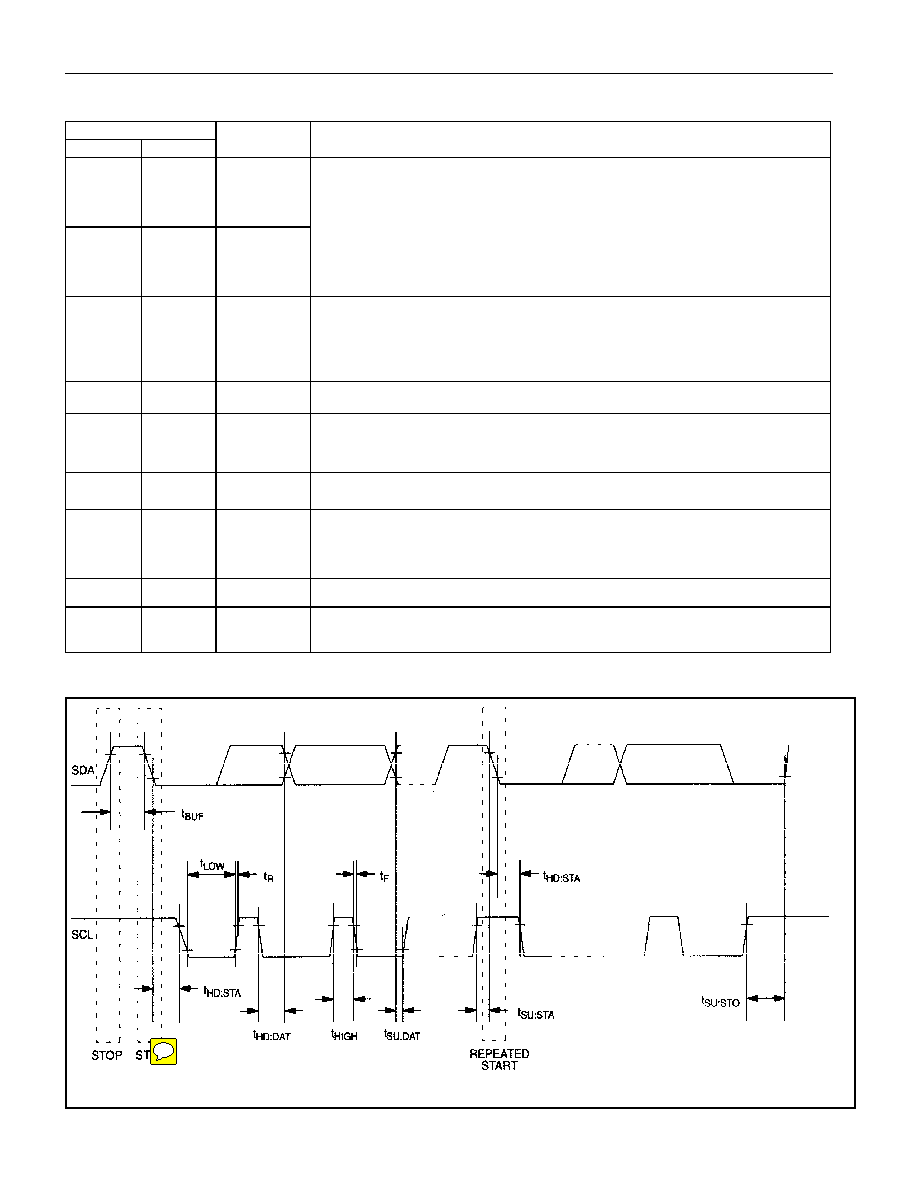
TIMING DIAGRAM
发布紧急采购,3分钟左右您将得到回复。
相关PDF资料
DS1338C-33#T&R
IC RTC 56BYTE NV SRAM 16SOIC
DS1339AU+
IC RTC I2C W/ALARM 8USOP
DS1339C-2#
IC RTC I2C W/ALARM 16-SOIC
DS1340Z-33/T&R
IC RTC I2C W/CHARGER 3.3V 8-SOIC
DS1340Z-3
IC RTC I2C W/CHARGER 3V 8-SOIC
DS1341T+
IC RTC I2C W/ALARM 6TDFN-EP
DS1344D-33+
IC RTC SPI 3.3V 14TDFN-EP
DS1347T+
IC RTC/CALENDAR SPI 8TDFN
相关代理商/技术参数
DS1337S+T&R
制造商:Maxim Integrated Products 功能描述:REAL TIME CLOCK SERL 8SOIC - Tape and Reel 制造商:Maxim Integrated Products 功能描述:SERIAL RTC 8P SOIC TRL LEADFREE 制造商:Maxim Integrated Products 功能描述:IC RTC SERIAL 2WIRE LP 8-SOIC 制造商:Maxim Integrated Products 功能描述:Real Time Clock I2C Serial RTC 制造商:Maxim Integrated Products 功能描述:Real Time Clock Serial SOIC8
DS1337S+T&R
功能描述:实时时钟 I2C Serial RTC RoHS:否 制造商:Microchip Technology 功能:Clock, Calendar. Alarm RTC 总线接口:I2C 日期格式:DW:DM:M:Y 时间格式:HH:MM:SS RTC 存储容量:64 B 电源电压-最大:5.5 V 电源电压-最小:1.8 V 最大工作温度:+ 85 C 最小工作温度: 安装风格:Through Hole 封装 / 箱体:PDIP-8 封装:Tube
DS1337U
功能描述:实时时钟 I2C Serial RTC RoHS:否 制造商:Microchip Technology 功能:Clock, Calendar. Alarm RTC 总线接口:I2C 日期格式:DW:DM:M:Y 时间格式:HH:MM:SS RTC 存储容量:64 B 电源电压-最大:5.5 V 电源电压-最小:1.8 V 最大工作温度:+ 85 C 最小工作温度: 安装风格:Through Hole 封装 / 箱体:PDIP-8 封装:Tube
DS1337U/T&R
制造商:Maxim Integrated Products 功能描述:REAL TIME CLOCK SERL 8USOP - Tape and Reel 制造商:Maxim Integrated Products 功能描述:IC RTC SERIAL 2WIRE LP 8-USOP 制造商:Maxim Integrated Products 功能描述:Real Time Clock I2C Serial RTC
DS1337U/T&R
功能描述:实时时钟 I2C Serial RTC RoHS:否 制造商:Microchip Technology 功能:Clock, Calendar. Alarm RTC 总线接口:I2C 日期格式:DW:DM:M:Y 时间格式:HH:MM:SS RTC 存储容量:64 B 电源电压-最大:5.5 V 电源电压-最小:1.8 V 最大工作温度:+ 85 C 最小工作温度: 安装风格:Through Hole 封装 / 箱体:PDIP-8 封装:Tube
DS1337U+
功能描述:实时时钟 I2C Serial RTC RoHS:否 制造商:Microchip Technology 功能:Clock, Calendar. Alarm RTC 总线接口:I2C 日期格式:DW:DM:M:Y 时间格式:HH:MM:SS RTC 存储容量:64 B 电源电压-最大:5.5 V 电源电压-最小:1.8 V 最大工作温度:+ 85 C 最小工作温度: 安装风格:Through Hole 封装 / 箱体:PDIP-8 封装:Tube
DS1337U+
制造商:Maxim Integrated Products 功能描述:SEMICONDUCTOR ((NW))
DS1337U+T&R
制造商:Maxim Integrated Products 功能描述:SERIAL RTC 8PIN USOP TRL LEADFREE 制造商:Maxim Integrated Products 功能描述:REAL TIME CLOCK SERL 8USOP - Tape and Reel 制造商:Maxim Integrated Products 功能描述:IC RTC SERIAL 2WIRE LP 8-USOP 制造商:Maxim Integrated Products 功能描述:Real Time Clock I2C Serial RTC